
Application of Microchip Lasers in Photoresist Repair
1. Photolithography Process
Photolithography machines are core equipment in the semiconductor industry, primarily used to fabricate microstructures on chips. They project patterns on photomasks onto silicon wafers and irradiate the wafer surface with ultraviolet light to form tiny microstructures[1].
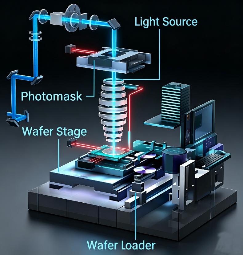
A lithography machine consists of three major modules: optical system, mechanical system and control system. Equipped with exposure light sources, lenses, reflectors and other optical components, the optical system projects micro-patterns on photomasks onto silicon wafer surfaces. The mechanical system includes workpiece stages, motion control systems, automatic alignment systems and other devices to precisely adjust the position and motion trajectory of silicon wafers. The control system is composed of computers and supporting control software to realize unified scheduling of the overall machine operating status and exposure procedures. Among the three modules, the optical system is the core component of the lithography machine. Meanwhile, exposure and development are the two most critical processes in the entire lithography workflow.
Exposure refers to the process of projecting photomask patterns onto silicon wafers through the optical system. Photoresists are divided into positive and negative types (the schematic of negative photoresist is on the left, and positive photoresist on the right)[1]. Positive photoresists undergo photochemical reactions under ultraviolet irradiation; the exposed areas can be dissolved by developer, and the finally retained patterns correspond to the light-shielded regions of the photomask. Negative photoresists crosslink under UV irradiation, making exposed areas resistant to dissolution by developer, and the reserved patterns match the transparent regions of the photomask.
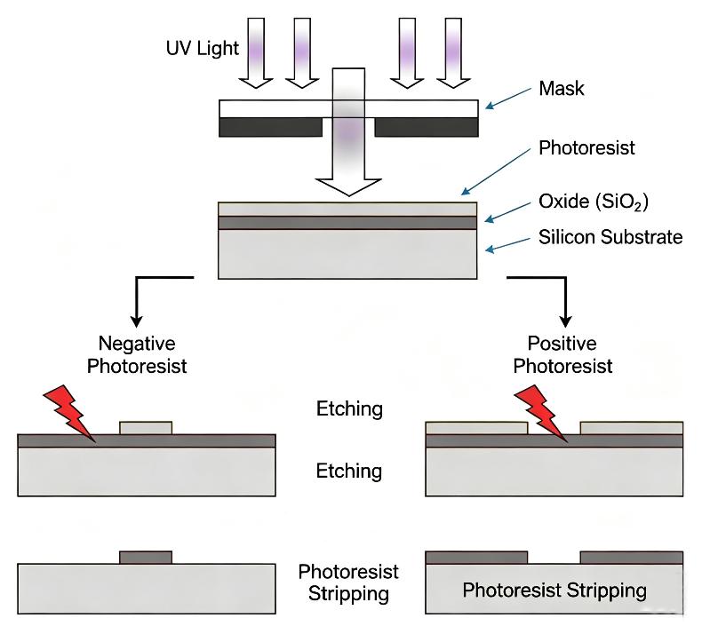
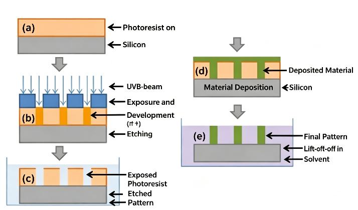
Development is a process that selectively dissolves photoresist with developer to form target patterns on the photoresist film. Developer is applied to the surface of exposed photoresist to selectively dissolve corresponding areas according to the photosensitive properties of photoresist. After cleaning and drying, patterned photoresist matching the photomask is formed. In the subsequent etching process, the photoresist acts as an etch barrier to etch the base film without photoresist protection, ultimately transferring patterns onto the wafer surface.
2. Photoresist Coating Methods and Resulting Defects
Both positive and negative photoresists play an irreplaceable role in lithography, so extremely high standards are required for photoresist coating.
There are four photoresist coating methods: manual coating, spin coating, spray coating and roll coating. Spin coating is the most widely used coating method at present, mainly due to the following advantages:
1. High coating uniformity; liquid can automatically penetrate capillary pores of experimental substrates.
2. Short coating time, enabling rapid mass preparation of samples.
3. Capable of forming single-layer coatings on thin sheet materials.
Photoresist spin coating is a key pretreatment process before pattern exposure. The uniformity of spin-coated films directly determines the execution effect of subsequent exposure processes and is a core factor affecting the molding quality of final lithographic patterns. The standard spin coating film-forming process is divided into three stages. First, the coating nozzle quantitatively sprays photoresist onto the center of the wafer. Then the wafer rotates at high speed, and centrifugal force spreads the central photoresist outward to the wafer edge, causing a bulge of accumulated photoresist at the edge. The thickness of photoresist film can be reduced by increasing the spin speed. Finally, the wafer keeps rotating at high speed, the solvent inside the film evaporates continuously, and a uniform and stable photoresist film is formed on the wafer surface.
Under conventional spin coating processes, the photoresist thickness along the wafer radius presents a typical “bowl-shaped” distribution: the film at the wafer center is slightly thicker, while the film in the middle area of the wafer is relatively uniform. Affected by centrifugal force and surface tension, obvious accumulated photoresist bulges (Edge Bead) form at the outermost edge of the wafer, and the edge film thickness is far higher than the standard film thickness. This radial fluctuation of film thickness will directly interfere with the focusing accuracy of subsequent lithography exposure and affect the stability of lithography processes. The thickness increase at the wafer center is slight and basically has no negative impact on exposure imaging. However, the problem of photoresist accumulation at the wafer edge is prominent, with thickness several times that of the standard process film. Excess residual photoresist at the edge easily spreads to the backside of the wafer, contaminates the wafer and affects the overall wafer process, as shown in the figure below.
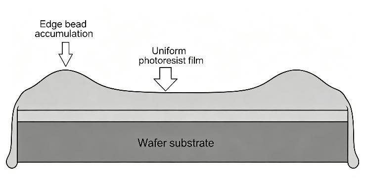
Excess photoresist on the edge and backside of the wafer will not only damage coating and developing equipment, but also interfere with exposure machines, and even contaminate equipment outside the lithography area. In view of these severe impacts, a special Edge Bead Removal (EBR) process is required to remove excess edge photoresist to complete lithography and protect production equipment. EBR operation can be carried out after the photoresist on the wafer cures into a stable film.
3. Photoresist Edge Repair
Two common EBR solutions are adopted in the industry for photoresist edge repair, with respective advantages and drawbacks.
3.1 Chemical EBR
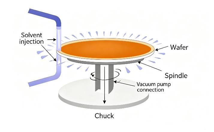
After coating and soft baking, Chemical EBR sprays edge removal solvents (PGMEA or EGMEA) onto the front, chamfer and back edge regions of the wafer. The coverage range of solvent must be strictly controlled during operation to avoid infiltration into the valid patterned area of photoresist[2]. This method dissolves edge films via solvent. In addition to stripping edge photoresist, it can simultaneously remove residual anti-reflective coating residues, process accumulated photoresist on the wafer front, chamfer and backside, and is compatible with all types of photoresists regardless of photosensitivity. However, fluid flow leads to uneven edge removal profiles, with hidden risks of solvent inward penetration damaging valid patterns. Dissolved photoresist debris easily causes particle contamination. Meanwhile, continuous consumption of high-purity organic solvents leads to relatively high costs for consumables and waste liquid treatment.
3.2 Optical EBR (Wafer Edge Exposure, WEE)
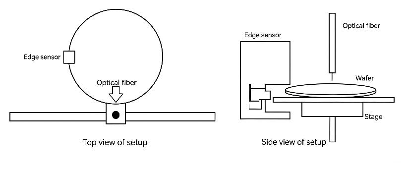
Optical EBR, also known as Wafer Edge Exposure (WEE), is arranged either after coating and soft baking before main pattern exposure, or after main pattern exposure. Lasers irradiate the wafer edge area to trigger photochemical reactions on the irradiated photoresist, which dissolves synchronously with exposed patterns in the subsequent development process[3]. Optical EBR requires no chemical solvents, maintains high cleanliness of the wafer surface, forms regular exposure boundaries, eliminates the risk of liquid-phase erosion on intact photoresist, and reduces single-wafer processing consumable costs. Its limitation lies in that it can only process photosensitive photoresists and cannot remove non-photosensitive anti-reflective coatings[4].
4. Optical Wafer Edge Exposure Process
The process stability of Optical EBR puts forward strict requirements for laser systems, and the selection of light source wavelength is critical. For mainstream i-line (365 nm) lithography processes, matched WEE schemes generally adopt 355 nm ultraviolet lasers. This wavelength matches the light absorption characteristics of commercial i-line photoresists well and can stably trigger target photochemical reactions. Meanwhile, 355 nm lasers feature mature industrialization, stable power output, low photoaging of optical components, and can reduce various defects induced by thin-film photodegradation and stray light. 266 nm deep ultraviolet lasers are only compatible with KrF (248 nm) photoresist systems and are not used for standard g/i-line processes. Direct matching with i-line photoresists will cause overexposure of the surface layer and insufficient photosensitivity of the bottom layer, leaving residual photoresist. In addition, lasers at this wavelength have low frequency-doubling conversion efficiency, limited service life of optical components, and a narrow overall process window.
To meet the light source demands of Optical EBR, RealLight independently developed the MCC series microchip lasers. The MCC RealSubns® microchip lasers feature ideal ultra-narrow pulse width and high single-pulse energy. As passively Q-switched diode pumped solid-state lasers, they deliver clean pulse waveforms without trailing pulses, stable single-pulse energy and excellent beam quality. The schematic diagram and physical photos are shown below.
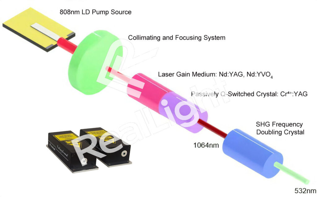
The laser adopts a passively Q-switched design with bonded Nd:YAG and Cr:YAG crystals, consistent with the proprietary microchip laser technical route of RealLight. We have profound technical accumulation in relevant processes, enabling long service life, high stability and wide-temperature operation. A thermoelectric cooler is built inside the laser to maintain a constant internal operating temperature, adapting to high and low temperature environments.
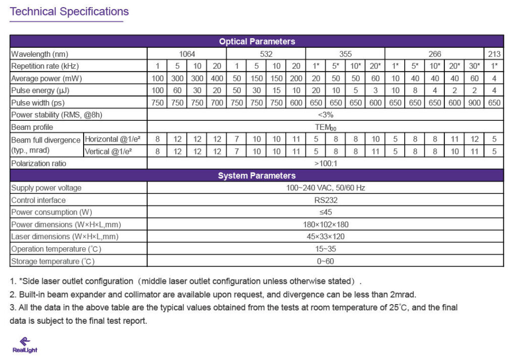
The MCC series covers five wavelengths: 1064 nm, 532 nm, 355 nm, 266 nm and 213 nm. Microchip lasers from RealLight support internal and external triggering. Synchronous control based on external trigger mode facilitates linkage with wafer rotation and positioning systems. Lasers at 355 nm and 266 nm support repetition rates of 1 kHz, 5 kHz, 10kHz and 20 kHz, with maximum single-pulse energy of 20 μJ and a pulse width of 650 ps. The technical parameter table of microchip lasers is shown below. Meanwhile, we provide customized high-repetition-rate 355 nm and 266 nm lasers for photoresist repair applications, with repetition rates up to 20 kHz or 30 kHz.
With the continuous advancement of semiconductor process nodes, market demand for wafer photoresist edge repair (EBR) grows steadily. Featuring high reliability, compact size and low cost, RealLight’s products will continuously empower the technical iteration of Wafer Edge Exposure (WEE). Optical EBR technology is expected to alleviate pollution and consumable pressure brought by chemical solvents, optimize process defects at wafer edges, and boost quality and reduce costs for lithography processes. We look forward to its further development.
RealLight is a high-tech enterprise focusing on the R&D, production and sales of semiconductor lasers, microchip lasers, erbium glass lasers, high-power solid-state lasers and supporting optical components. Based on independent innovation, the company provides high-performance, high-reliability and customizable laser light sources and system solutions for radar ranging, analytical instruments, biomedicine, scientific research and laser processing fields, and supports one-stop OEM/ODM customization and development services.
Disclaimer
Part of the content of this document is sourced from the internet, intended only for technical research and communication, for reference and study. Please feel free to put forward suggestions if there are descriptive or academic errors. If any copyright issues are involved, contact us for verification and deletion as soon as possible.
References
[1] icguide. Step-by-Step Guide to the Working Principle of Lithography Machines [EB/OL]. 2024-04-12.
[2] Laura Peters. Edge Treatment Is Critical for Hard Masks[J]. Integrated Circuit Applications, 2007(10):29.
[3] Detailed Explanation of Semiconductor Photolithography Process. Electronic Fans. 2025-11-10.
[4] Wei Yiyi. Advanced Lithography Theory and Applications for VLSI. Beijing: Science Press, 2016:35-36, 39-40.





 777
777