
Ideal Light Source for Photoresist Edge Bead Removal (EBR/WEE)
1. Industry Background: The Need for Photoresist Edge Repair
When applying photoresist on wafers through spin coating, the adhesive material accumulates and thickens at the edges and the backside due to centrifugal force, forming “edge beads” (Edge Bead), which are prone to peeling off, causing particles and triggering abnormal patterns. Therefore, edge bead removal (EBR) must be performed after the soft baking of the coating and before the main exposure.
Chemical EBR uses solvent spraying, which is prone to contamination and material consumption; optical EBR/WEE uses ultraviolet laser exposure on the edge film of the photoresist, dissolving simultaneously during development, without solvents, with well-defined contours, high cleanliness, and low cost. It is an advanced process direction. If the edge beads are not removed, they will transfer to pattern defects in subsequent exposure and etching, directly reducing wafer yield. The wavelength must match the photoresist: i-line (365nm) process uses 355nm, KrF (248nm) uses 266nm. This ultraviolet light source has long relied on imports, and domestic alternatives are accelerating.
2. Principle of Photoresist Repair
The principle of optical EBR/WEE is as follows: After the wafer is coated with adhesive and undergoes a gentle soft baking process, a high-energy ultraviolet laser is used to scan the “edge beads” areas on the edges and the backside of the wafer. The ultraviolet photons have high energy (355nm ≈ 3.49 eV, 266nm ≈ 4.66 eV), and after being absorbed by the photosensitive groups of the photoresist, they directly undergo photochemical reactions, converting the originally insoluble edge adhesive film into soluble; during the subsequent development process, the irradiated edge adhesive film dissolves synchronously with the main exposure pattern, thereby precisely removing the edge beads.
During the exposure process, the wafer rotates at a constant speed, and the laser beam is positioned by an edge sensor and scans in a circular manner along the edge to ensure the precise position of the exposure band and uniform dose. Since it mainly relies on photochemical “cold processing”, the heat affected zone is extremely small, which neither damages the glass/silicon substrate nor affects the adjacent normal photolithography patterns.
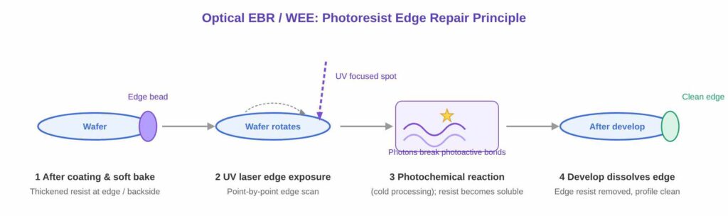
Fig. 1 Principle of the optical EBR/WEE photoresist edge repair process
3. Light Source Requirements for Photoresist Repair
The optical EBR has strict requirements for the light source: the wavelength must match the absorption of the photomask (355/266nm); the pulse should be short to reduce the thermal affected zone; the repetition frequency should be high enough to coordinate with the high-speed rotation of the wafer for point-by-point exposure; the focused spot size must be controlled at the micrometer level to precisely define the exposure boundary, and the energy does not drift under high repetition frequency; the beam TEM₀₀ supports external triggering and synchronizes with the rotating positioning system; the entire machine is compact and has a long lifespan. Traditional imported nanosecond DPSS has a pulse width of 5–10ns, with large heat impact, large volume, long lead time, and high cost.
4. RealLight’s MCC Series Microchip Laser
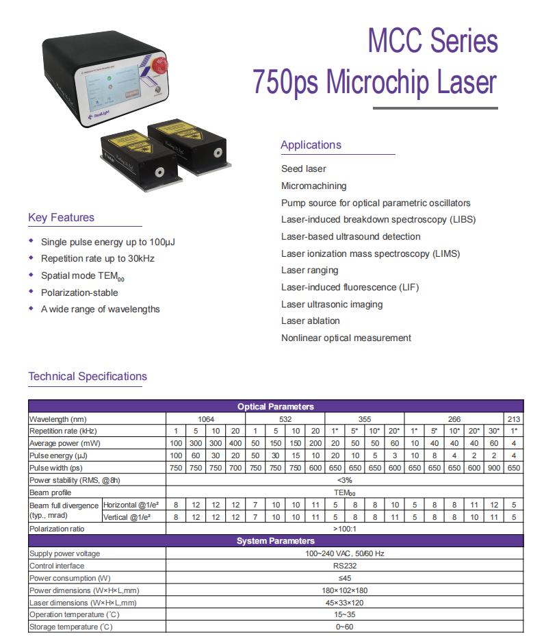
RealLight’s MCC series is a diode-pumped, passively Q-switched solid-state microchip laser: an 808nm diode pumps the Nd:YAG gain medium which, together with the bonded Cr⁴⁺:YAG saturable absorber, model-locks narrow 1064nm pulses; nonlinear crystals then double / sum-frequency them into 355nm (third harmonic) and 266nm (fourth harmonic). The 355nm version runs at 1/5/10/20kHz, while 266nm reaches 30kHz; the pulse width is 650–750ps, the single-pulse energy is up to 20μJ; the TEM₀₀ beam, the polarization ratio is >100:1; the power stability is <3% RMS; it supports internal/external triggering and can be linked with the wafer rotation system; the integrated sealed laser head is only 45×33×120mm.
| Parameter | 355nm Version | 266nm Version |
| Wavelength | 355nm (3rd harmonic) | 266nm (4th harmonic) |
| Available repetition rates | 1/5/10/20kHz | 1/5/10/20/30kHz |
| Pulse width | 650–750ps | 650–750ps |
| Single-pulse energy | Up to ~20μJ | Up to ~10μJ |
| Trigger / stability | External trigger sync | <3% RMS | External trigger sync | <3% RMS |
Note: typical values; final specifications are subject to the factory test report.
5. Core Advantages of the MCC Series
· Sub-nanosecond cold processing: 650–750 ps is much shorter than traditional nanosecond light sources. The heat affected zone is smaller, the edge profile is sharp, and residual glue and overexposure are reduced.
· Clean, tail-free pulses: The front edge is steep, the rear edge is clean, the single pulse dose is precise, and the exposure consistency is high.
· TEM₀₀ high beam quality: The focused spot is small, the exposure bandwidth is precisely controlled, and adjacent patterns are not damaged.
· High 20/30kHz repetition rate: 266 nm reaches 30 kHz. Combined with high-speed rotating wafer point-by-point exposure, it balances uniformity and production capacity.
· External trigger sync: Linked with rotational positioning; 355 nm is paired with i-line, 266 nm is paired with KrF, covering mainstream processes.
· Compact, easy to integrate & domestic substitution: The OEM laser head is small, the TEC maintains constant temperature and has a long lifespan; self-production, delivery time, cost and after-sales are better.
For more product information, please contact the RealLight sales team!
Disclaimer: Part of the content in this document is sourced online, intended solely for technical-research exchange and reference purposes. Feedback is welcome for factual or academic errors. Should any copyright concerns arise, please contact us for prompt verification and removal.
References





 777